1. Product Principles and Architectural Characteristics of Alumina Ceramics
1.1 Crystallographic and Compositional Basis of α-Alumina
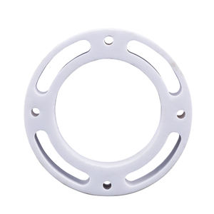
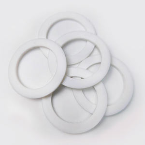
(Alumina Ceramic Substrates)
Alumina ceramic substratums, mostly made up of light weight aluminum oxide (Al two O FOUR), serve as the backbone of modern-day digital product packaging because of their exceptional equilibrium of electrical insulation, thermal stability, mechanical stamina, and manufacturability.
One of the most thermodynamically secure stage of alumina at heats is corundum, or α-Al ₂ O THREE, which takes shape in a hexagonal close-packed oxygen latticework with aluminum ions inhabiting two-thirds of the octahedral interstitial websites.
This dense atomic arrangement conveys high hardness (Mohs 9), superb wear resistance, and solid chemical inertness, making α-alumina ideal for severe operating atmospheres.
Commercial substratums typically contain 90– 99.8% Al Two O TWO, with minor additions of silica (SiO ₂), magnesia (MgO), or unusual earth oxides made use of as sintering help to advertise densification and control grain growth during high-temperature processing.
Higher pureness grades (e.g., 99.5% and above) show remarkable electric resistivity and thermal conductivity, while reduced pureness versions (90– 96%) supply economical remedies for less requiring applications.
1.2 Microstructure and Issue Engineering for Electronic Reliability
The efficiency of alumina substrates in electronic systems is critically dependent on microstructural harmony and defect minimization.
A penalty, equiaxed grain framework– commonly varying from 1 to 10 micrometers– ensures mechanical honesty and reduces the probability of crack proliferation under thermal or mechanical anxiety.
Porosity, particularly interconnected or surface-connected pores, have to be minimized as it deteriorates both mechanical strength and dielectric performance.
Advanced handling methods such as tape spreading, isostatic pushing, and controlled sintering in air or regulated environments allow the manufacturing of substrates with near-theoretical thickness (> 99.5%) and surface area roughness below 0.5 µm, necessary for thin-film metallization and cord bonding.
Furthermore, impurity segregation at grain limits can lead to leak currents or electrochemical movement under bias, necessitating rigorous control over basic material pureness and sintering problems to ensure long-lasting reliability in damp or high-voltage environments.
2. Manufacturing Processes and Substratum Manufacture Technologies
( Alumina Ceramic Substrates)
2.1 Tape Casting and Green Body Processing
The manufacturing of alumina ceramic substrates begins with the prep work of a highly distributed slurry consisting of submicron Al ₂ O five powder, organic binders, plasticizers, dispersants, and solvents.
This slurry is refined via tape spreading– a continual method where the suspension is spread over a moving carrier movie utilizing a precision physician blade to accomplish uniform density, generally between 0.1 mm and 1.0 mm.
After solvent dissipation, the resulting “eco-friendly tape” is adaptable and can be punched, drilled, or laser-cut to create by means of holes for upright affiliations.
Multiple layers may be laminated to create multilayer substratums for complex circuit assimilation, although the majority of industrial applications utilize single-layer setups due to set you back and thermal growth considerations.
The green tapes are then very carefully debound to remove organic additives through managed thermal decay prior to last sintering.
2.2 Sintering and Metallization for Circuit Combination
Sintering is conducted in air at temperature levels between 1550 ° C and 1650 ° C, where solid-state diffusion drives pore elimination and grain coarsening to accomplish complete densification.
The direct contraction throughout sintering– normally 15– 20%– must be exactly anticipated and made up for in the style of eco-friendly tapes to guarantee dimensional accuracy of the last substratum.
Following sintering, metallization is applied to create conductive traces, pads, and vias.
2 primary approaches control: thick-film printing and thin-film deposition.
In thick-film innovation, pastes having steel powders (e.g., tungsten, molybdenum, or silver-palladium alloys) are screen-printed onto the substratum and co-fired in a lowering environment to develop robust, high-adhesion conductors.
For high-density or high-frequency applications, thin-film processes such as sputtering or evaporation are used to down payment adhesion layers (e.g., titanium or chromium) adhered to by copper or gold, enabling sub-micron patterning using photolithography.
Vias are filled with conductive pastes and terminated to develop electrical interconnections between layers in multilayer layouts.
3. Practical Qualities and Performance Metrics in Electronic Systems
3.1 Thermal and Electrical Habits Under Functional Stress And Anxiety
Alumina substratums are prized for their favorable mix of moderate thermal conductivity (20– 35 W/m · K for 96– 99.8% Al Two O TWO), which makes it possible for reliable warm dissipation from power tools, and high volume resistivity (> 10 ¹⁴ Ω · centimeters), making sure very little leakage current.
Their dielectric consistent (εᵣ ≈ 9– 10 at 1 MHz) is steady over a vast temperature and frequency variety, making them appropriate for high-frequency circuits up to several ghzs, although lower-κ products like light weight aluminum nitride are preferred for mm-wave applications.
The coefficient of thermal growth (CTE) of alumina (~ 6.8– 7.2 ppm/K) is fairly well-matched to that of silicon (~ 3 ppm/K) and certain product packaging alloys, minimizing thermo-mechanical tension during device procedure and thermal cycling.
Nevertheless, the CTE mismatch with silicon remains a problem in flip-chip and direct die-attach setups, frequently requiring certified interposers or underfill products to mitigate exhaustion failing.
3.2 Mechanical Robustness and Ecological Resilience
Mechanically, alumina substratums show high flexural stamina (300– 400 MPa) and superb dimensional stability under tons, enabling their use in ruggedized electronics for aerospace, automobile, and commercial control systems.
They are immune to resonance, shock, and creep at elevated temperature levels, keeping architectural honesty approximately 1500 ° C in inert environments.
In damp atmospheres, high-purity alumina shows minimal dampness absorption and outstanding resistance to ion migration, making sure long-term reliability in outdoor and high-humidity applications.
Surface solidity additionally protects against mechanical damage during handling and setting up, although treatment should be taken to avoid edge chipping as a result of fundamental brittleness.
4. Industrial Applications and Technological Influence Throughout Sectors
4.1 Power Electronics, RF Modules, and Automotive Equipments
Alumina ceramic substrates are common in power electronic components, consisting of insulated entrance bipolar transistors (IGBTs), MOSFETs, and rectifiers, where they give electrical isolation while assisting in warmth transfer to warm sinks.
In superhigh frequency (RF) and microwave circuits, they serve as carrier platforms for crossbreed incorporated circuits (HICs), surface area acoustic wave (SAW) filters, and antenna feed networks due to their stable dielectric residential or commercial properties and reduced loss tangent.
In the automotive industry, alumina substrates are made use of in engine control units (ECUs), sensing unit plans, and electrical vehicle (EV) power converters, where they withstand high temperatures, thermal cycling, and exposure to destructive fluids.
Their dependability under extreme problems makes them indispensable for safety-critical systems such as anti-lock braking (ABDOMINAL) and progressed driver support systems (ADAS).
4.2 Medical Tools, Aerospace, and Emerging Micro-Electro-Mechanical Solutions
Beyond consumer and commercial electronics, alumina substratums are employed in implantable medical gadgets such as pacemakers and neurostimulators, where hermetic securing and biocompatibility are paramount.
In aerospace and protection, they are utilized in avionics, radar systems, and satellite communication components as a result of their radiation resistance and security in vacuum cleaner environments.
Additionally, alumina is increasingly made use of as a structural and insulating platform in micro-electro-mechanical systems (MEMS), consisting of stress sensors, accelerometers, and microfluidic gadgets, where its chemical inertness and compatibility with thin-film handling are useful.
As digital systems remain to demand greater power thickness, miniaturization, and reliability under severe conditions, alumina ceramic substrates stay a foundation product, linking the void in between performance, price, and manufacturability in advanced digital packaging.
5. Vendor
Alumina Technology Co., Ltd focus on the research and development, production and sales of aluminum oxide powder, aluminum oxide products, aluminum oxide crucible, etc., serving the electronics, ceramics, chemical and other industries. Since its establishment in 2005, the company has been committed to providing customers with the best products and services. If you are looking for high quality alumina carbon refractory, please feel free to contact us. (nanotrun@yahoo.com)
Tags: Alumina Ceramic Substrates, Alumina Ceramics, alumina
All articles and pictures are from the Internet. If there are any copyright issues, please contact us in time to delete.
Inquiry us